- 您现在的位置:买卖IC网 > Sheet目录492 > NTR4171PT3G (ON Semiconductor)MOSFET P-CH 30V 2.2A SOT23-3
�� �
�
�NTR4171P�
�Power� MOSFET�
�?� 30� V,� ?� 3.5� A,� Single� P� ?� Channel,� SOT� ?� 23�
�Features�
�?� Low� R� DS(on)� at� Low� Gate� Voltage�
�?� Low� Threshold� Voltage�
�?� High� Power� and� Current� Handling� Capability�
�?� This� is� a� Pb� ?� Free� Device�
�Applications�
�?� Load� Switch�
�?� Optimized� for� Battery� and� Load� Management� Applications� in�
�Portable� Equipment� like� Cell� Phones,� PDA’s,� Media� Players,� etc.�
�V� (BR)DSS�
�?� 30� V�
�http://onsemi.com�
�R� DS(on)� MAX�
�75� m� W� @� ?� 10� V�
�110� m� W� @� ?� 4.5� V�
�150� m� W� @� ?� 2.5� V�
�I� D� MAX�
�?� 2.2� A�
�?� 1.8� A�
�?� 1.0� A�
�MAXIMUM� RATINGS� (T� J� =� 25� °� C� unless� otherwise� noted)�
�Parameter� Symbol�
�Value�
�Unit�
�P� ?� CHANNEL� MOSFET�
�S�
�Drain� ?� to� ?� Source� Voltage�
�Gate� ?� to� ?� Source� Voltage�
�V� DSS�
�V� GS�
�?� 30�
�±� 12�
�V�
�V�
�Continuous� Drain�
�Current� (Note� 1)�
�Steady�
�State�
�T� A� =� 25� °� C�
�T� A� =� 85� °� C�
�I� D�
�?� 2.2�
�?� 1.5�
�A�
�G�
�t� ≤� 5s�
�T� A� =� 25� °� C�
�?� 3.5�
�D�
�Power� Dissipation�
�(Note� 1)�
�Steady�
�State�
�t� ≤� 5s�
�T� A� =� 25� °� C�
�P� D�
�0.48�
�1.25�
�W�
�3�
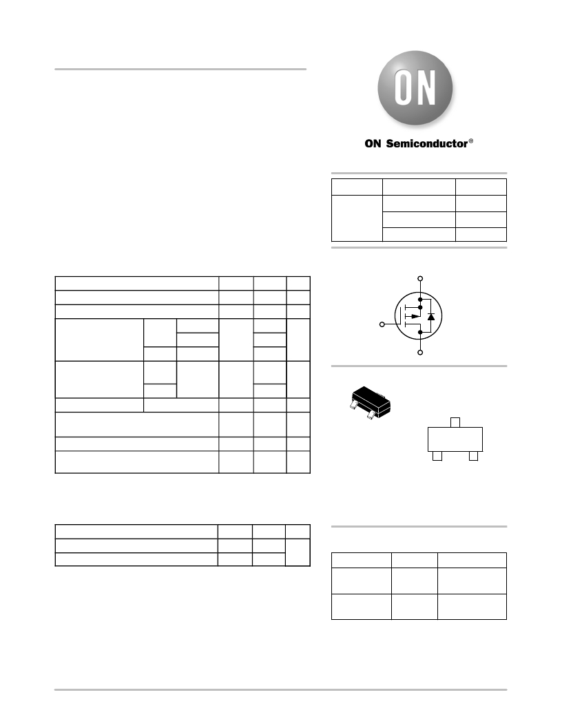
�MARKING� DIAGRAM/�
�PIN� ASSIGNMENT�
�Pulsed� Drain� Current� t� p� =� 10� m� s�
�Operating� Junction� and� Storage� Temperature�
�Source� Current� (Body� Diode)�
�I� DM�
�T� J� ,�
�T� stg�
�I� S�
�?� 15.0�
�?� 55� to�
�150�
�?� 1.0�
�A�
�°� C�
�A�
�1�
�2�
�SOT� ?� 23�
�CASE� 318�
�3�
�Drain�
�TRFM� G�
�G�
�Lead� Temperature� for� Soldering� Purposes�
�(1/8� ″� from� case� for� 10� s)�
�T� L�
�260�
�°� C�
�STYLE� 21�
�1�
�Gate�
�2�
�Source�
�Stresses� exceeding� Maximum� Ratings� may� damage� the� device.� Maximum�
�Ratings� are� stress� ratings� only.� Functional� operation� above� the� Recommended�
�Operating� Conditions� is� not� implied.� Extended� exposure� to� stresses� above� the�
�Recommended� Operating� Conditions� may� affect� device� reliability.�
�THERMAL� RESISTANCE� RATINGS�
�TRF� =� Specific� Device� Code�
�M� =� Date� Code�
�G� =� Pb� ?� Free� Package�
�(Note:� Microdot� may� be� in� either� location)�
�Parameter�
�Symbol�
�Max�
�Unit�
�Junction� ?� to� ?� Ambient� ?� Steady� State� (Note� 1)�
�R� q� JA�
�260�
�°� C/W�
�ORDERING� INFORMATION�
�Junction� ?� to� ?� Ambient� ?� t� ≤� 10� s� (Note� 1)�
�R� q� JA�
�100�
�Device�
�Package�
�Shipping� ?�
�1.� Surface� ?� mounted� on� FR4� board� using� 1� in� sq� pad� size� (Cu� area� =� 1.127� in� sq�
�[2� oz]� including� traces)�
�NTR4171PT1G�
�NTR4171PT3G�
�SOT� ?� 23�
�(Pb� ?� Free)�
�SOT� ?� 23�
�3000/Tape� &� Reel�
�10000/Tape� &� Reel�
�(Pb� ?� Free)�
�?For� information� on� tape� and� reel� specifications,�
�including� part� orientation� and� tape� sizes,� please�
�refer� to� our� Tape� and� Reel� Packaging� Specification�
�Brochure,� BRD8011/D.�
�?� Semiconductor� Components� Industries,� LLC,� 2010�
�May,� 2010� ?� Rev.� 1�
�1�
�Publication� Order� Number:�
�NTR4171P/D�
�发布紧急采购,3分钟左右您将得到回复。
相关PDF资料
NTR4501NT1
MOSFET N-CHAN 3.2A 20V SOT-23
NTR4502PT1G
MOSFET P-CH 30V 1.13A SOT-23
NTR4503NT3G
MOSFET N-CH 30V 1.5A SOT-23
NTS2101PT1
MOSFET P-CH 8V 1.4A SOT-323
NTS4001NT1
MOSFET N-CH 30V 270MA SOT-323
NTS4101PT1
MOSFET P-CH 20V 1.37A SOT-323
NTS4172NT1G
MOSFET N-CH 30V 1.6A SC70-3
NTS4173PT1G
MOSFET P-CH 30V 1.2A SC70-3
相关代理商/技术参数
NTR4501N
制造商:ONSEMI 制造商全称:ON Semiconductor 功能描述:Power MOSFET 20 V, 3.2 A, Single N−Channel, SOT−23
NTR4501NST1G
制造商:ON Semiconductor 功能描述:NFET SOT23 20V 3.2A 80MO - Tape and Reel 制造商:ON Semiconductor 功能描述:MOSFET NFET SOT23 20V 3.2A 80MO 制造商:ON Semiconductor 功能描述:REEL / NFET SOT23 20V 3.2A 80MO
NTR4501NT1
功能描述:MOSFET 20V 3.2A N-Channel RoHS:否 制造商:STMicroelectronics 晶体管极性:N-Channel 汲极/源极击穿电压:650 V 闸/源击穿电压:25 V 漏极连续电流:130 A 电阻汲极/源极 RDS(导通):0.014 Ohms 配置:Single 最大工作温度: 安装风格:Through Hole 封装 / 箱体:Max247 封装:Tube
NTR4501NT1G
功能描述:MOSFET 20V 3.2A N-Channel RoHS:否 制造商:STMicroelectronics 晶体管极性:N-Channel 汲极/源极击穿电压:650 V 闸/源击穿电压:25 V 漏极连续电流:130 A 电阻汲极/源极 RDS(导通):0.014 Ohms 配置:Single 最大工作温度: 安装风格:Through Hole 封装 / 箱体:Max247 封装:Tube
NTR4501NT1G-CUT TAPE
制造商:ON 功能描述:NTR Series N-Channel 20 V 70 mOhm 1.25 W Surface Mount Power MOSFET - SOT-23
NTR4501NT3
功能描述:MOSFET 20V 3.2A N-Channel RoHS:否 制造商:STMicroelectronics 晶体管极性:N-Channel 汲极/源极击穿电压:650 V 闸/源击穿电压:25 V 漏极连续电流:130 A 电阻汲极/源极 RDS(导通):0.014 Ohms 配置:Single 最大工作温度: 安装风格:Through Hole 封装 / 箱体:Max247 封装:Tube
NTR4501NT3G
功能描述:MOSFET 20V 3.2A N-Channel RoHS:否 制造商:STMicroelectronics 晶体管极性:N-Channel 汲极/源极击穿电压:650 V 闸/源击穿电压:25 V 漏极连续电流:130 A 电阻汲极/源极 RDS(导通):0.014 Ohms 配置:Single 最大工作温度: 安装风格:Through Hole 封装 / 箱体:Max247 封装:Tube
NTR4501NT3H
制造商:Rochester Electronics LLC 功能描述: 制造商:ON Semiconductor 功能描述: